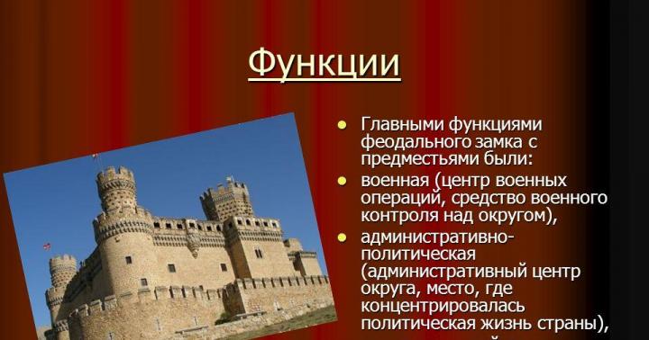
Printed circuit board(English printed circuit board, PCB, or printed wiring board, PWB) - a dielectric plate, on the surface and / or in the volume of which electrically conductive circuits of an electronic circuit are formed. The printed circuit board is designed for electrical and mechanical connection of various electronic components. Electronic components on a printed circuit board are connected with their leads to the elements of the conductive pattern, usually by soldering.
In contrast to surface mounting, on a printed circuit board, the electrically conductive pattern is made of foil, entirely located on a solid insulating base. The printed circuit board contains mounting holes and pads for mounting pin or planar components. In addition, printed circuit boards have vias for electrical connection of foil sections located on different layers of the board. From the outside, the board is usually coated with a protective coating (“solder mask”) and markings (an auxiliary figure and text according to the design documentation).
Depending on the number of layers with an electrically conductive pattern, printed circuit boards are divided into:
- single-sided (SPP): there is only one layer of foil glued to one side of the dielectric sheet.
- double-sided (DPP): two layers of foil.
- multilayer (MPP): foil not only on two sides of the board, but also in the inner layers of the dielectric. Multilayer printed circuit boards are obtained by gluing several single-sided or double-sided boards.
As the complexity of the designed devices and the density of mounting increases, the number of layers on the boards increases]. According to the properties of the base material:
- Rigid
- Thermally conductive
- Flexible
Printed circuit boards may have their own characteristics, due to their purpose and requirements for special operating conditions (for example, extended temperature range) or application features (for example, boards for devices operating at high frequencies).
materials The basis of the printed circuit board is a dielectric, the most commonly used materials are fiberglass, getinaks. Also, a metal base coated with a dielectric (for example, anodized aluminum) can serve as the basis for printed circuit boards; copper foil tracks are applied over the dielectric. Such printed circuit boards are used in power electronics for efficient heat removal from electronic components. In this case, the metal base of the board is attached to the radiator. As a material for printed circuit boards operating in the microwave range and at temperatures up to 260 ° C, fluoroplastic reinforced with glass fabric (for example, FAF-4D) and ceramics are used.
Flexible boards are made from polyimide materials such as Kapton.
Getinaks used under medium operating conditions.
- Pros: Cheap, less drilling, hot integration.
- Disadvantages: can delaminate during machining, can absorb moisture, lowers its dielectric properties and warps.
It is better to use getinax lined with electroplating foil.
Foil fiberglass- obtained by pressing, impregnation epoxy resin layers of fiberglass and glued surface film VF-4R of copper electrical foil with a thickness of 35-50 microns.
- Advantages: good dielectric properties.
- Disadvantages: expensive by 1.5-2 times.
Used for single-sided and double-sided boards. For multilayer PCBs, thin foil dielectrics FDM-1, FDM-2 and semi-flexible RDME-1 are used. The basis of such materials is an impregnating epoxy layer of fiberglass. Thickness of electrotechnical copper of electrotechnical foil is 35.18 microns. For the manufacture of multilayer PP, a cushioning fabric is used, for example, SPT-2 with a thickness of 0.06-0.08 mm, which is a non-foil material.
Manufacturing The production of PP is possible by an additive or subtractive method. In the additive method, a conductive pattern is formed on a non-foiled material by chemical copper plating through a protective mask previously applied to the material. In the subtractive method, a conductive pattern is formed on a foil material by removing unnecessary sections of the foil. AT modern industry only the subtractive method is used.
The whole PCB manufacturing process can be divided into four stages:
- Production of blanks (foil material).
- Processing the workpiece in order to obtain the desired electrical and mechanical appearance.
- Assembly of components.
- Testing.
Often, the production of printed circuit boards is understood only as the processing of a workpiece (foil material). A typical process for processing a foil material consists of several stages: drilling vias, obtaining a pattern of conductors by removing excess copper foil, plating holes, applying protective coatings and tinning, and marking. For multilayer printed circuit boards, pressing the final board from several blanks is added.
foil material- a flat sheet of dielectric with copper foil glued to it. As a rule, fiberglass is used as a dielectric. In old or very cheap equipment, textolite is used on fabric or paper basis, sometimes referred to as getinax. Fluorine-containing polymers (fluoroplastics) are used in microwave devices. The thickness of the dielectric is determined by the required mechanical and electrical strength, the most widely used thickness is 1.5 mm. A continuous sheet of copper foil is glued onto the dielectric on one or both sides. The thickness of the foil is determined by the currents for which the board is designed. The most widely used foil is 18 and 35 microns thick, 70, 105 and 140 microns are much less common. These values are based on standard copper thicknesses in imported materials, in which the thickness of the copper foil layer is calculated in ounces (oz) per square foot. 18 microns corresponds to ½ oz and 35 microns to 1 oz.
 Aluminum printed circuit boards A separate group of materials are aluminum metal printed circuit boards.] They can be divided into two groups.
- The first group is solutions in the form of an aluminum sheet with a high-quality oxidized surface, on which copper foil is glued. Such boards cannot be drilled, so they are usually made only one-sided. Processing of such foil materials is carried out according to traditional technologies of chemical drawing. Sometimes instead of aluminum, copper or steel is used, laminated with a thin insulator and foil. Copper has a high thermal conductivity, stainless steel board provides corrosion resistance.
- The second group involves the creation of a conductive pattern directly in the base aluminum. For this purpose, the aluminum sheet is oxidized not only over the surface, but also to the entire depth of the base, according to the pattern of conductive regions specified by the photomask.
Obtaining a drawing of conductors In the manufacture of boards, chemical, electrolytic or mechanical methods are used to reproduce the required conductive pattern, as well as their combinations.
The chemical method of manufacturing printed circuit boards from finished foil material consists of two main stages: applying a protective layer to the foil and etching unprotected areas by chemical methods. In industry, the protective layer is applied by photolithography using an ultraviolet-sensitive photoresist, a photomask and a UV light source. The photoresist completely covers the copper of the foil, after which the pattern of tracks from the photomask is transferred to the photoresist by illumination. The exposed photoresist is washed away, exposing the copper foil for etching, while the unexposed photoresist is fixed to the foil, protecting it from etching.
Photoresist can be liquid or film. Liquid photoresist is applied in industrial conditions, as it is sensitive to non-compliance with the application technology. Film photoresist is popular for handmade boards, but is more expensive. A photomask is a UV-transparent material with a track pattern printed on it. After exposure, the photoresist is developed and fixed as in a conventional photochemical process. In amateur conditions, a protective layer in the form of varnish or paint can be applied by silk screening or by hand. To form an etching mask on a foil, radio amateurs use the transfer of toner from an image printed on a laser printer (“laser-ironing technology”). Foil etching is the chemical process of converting copper into soluble compounds. Unprotected foil is etched, most often, in a solution of ferric chloride or in a solution of other chemicals, such as copper sulphate, ammonium persulfate, ammonia copper chloride, ammonia copper sulfate, based on chlorites, based on chromic anhydride. When using ferric chloride, the board etching process proceeds as follows: FeCl3+Cu → FeCl2+CuCl. Typical solution concentration 400 g/l, temperature up to 35°C. When using ammonium persulfate, the board etching process proceeds as follows: (NH4)2S2O8+Cu → (NH4)2SO4+CuSO4]. After etching, the protective pattern is washed off the foil.
mechanical method manufacturing involves the use of milling and engraving machines or other tools for the mechanical removal of a layer of foil from specified areas.
Until recently laser engraving printed circuit boards was poorly distributed due to the good reflective properties of copper at the wavelength of the most common high-power CO gas lasers. In connection with the progress in the field of laser engineering, industrial prototyping facilities based on lasers have now begun to appear.
Hole plating Transition and mounting holes can be drilled, punched mechanically (in soft materials such as getinaks) or lasered (very thin vias). Hole plating is usually done chemically or mechanically.
Mechanical plating of holes is carried out with special rivets, soldered wires or by filling the hole with conductive glue. The mechanical method is expensive to manufacture and therefore is used extremely rarely, usually in highly reliable piece solutions, special high-current equipment or amateur radio conditions.
During chemical metallization, holes are first drilled in a foil blank, then they are metallized, and only then the foil is etched to obtain a print pattern. Chemical plating of holes is a multi-stage complex process, sensitive to the quality of reagents and compliance with the technology. Therefore, it is practically not used in amateur radio conditions. Simplified, it consists of the following steps:
- Deposition of a conductive substrate on the dielectric walls of the hole. This pad is very thin and not durable. Applied by chemical metal deposition from unstable compounds such as palladium chloride.
- Copper is electrolytically or chemically deposited onto the resulting base.
In the end production cycle to protect the rather loose deposited copper, either hot tinning is used, or the hole is protected with varnish (solder mask). Untinned, poor quality vias are one of the most common causes of failure in electronics.
Multilayer boards (with more than 2 metallization layers) are assembled from a stack of thin two- or single-layer printed circuit boards made in the traditional way (except for the outer layers of the package - they are still left with intact foil). They are assembled as a "sandwich" with special gaskets (prepregs). Next, pressing in an oven, drilling and plating of vias is performed. Lastly, the foil of the outer layers is etched.
Via holes in such boards can also be made prior to pressing. If the holes are made before pressing, then it is possible to obtain boards with so-called blind holes (when there is a hole in only one layer of the sandwich), which makes it possible to compact the layout.
Covers such as:
- Protective and decorative varnish coatings ("solder mask"). Usually has a characteristic green color. When choosing a solder mask, keep in mind that some of them are opaque and you can't see the conductors under them.
- Decorative and informational coatings (marking). It is usually applied by silk screen printing, less often by inkjet or laser.
- Tinning of conductors. Protects the copper surface, increases the thickness of the conductor, facilitates the installation of components. Usually done by dipping into a solder bath or solder wave. The main disadvantage is the significant thickness of the coating, which makes it difficult to install high-density components. To reduce the thickness, excess solder during tinning is blown off with an air stream.
- Chemical, immersion or galvanic coating of conductor foil with inert metals (gold, silver, palladium, tin, etc.). Some types of such coatings are applied before the copper etching stage.
- Coating with conductive varnishes to improve the contact properties of connectors and membrane keypads or to create an additional layer of conductors.
After mounting printed circuit boards, it is possible to apply additional protective coatings that protect both the board itself and the soldering and components.
Mechanical restoration Many individual boards are often placed on one blank sheet. They go through the entire process of processing a foil blank as one board, and only at the end they are prepared for separation. If the boards are rectangular, then non-through grooves are milled, which facilitate the subsequent breaking of the boards (scribing, from the English scribe to scratch). If the boards are of complex shape, then through milling is done, leaving narrow bridges so that the boards do not crumble. For boards without plating, instead of milling, a series of holes with a small pitch is sometimes drilled. Drilling of mounting (non-plated) holes also occurs at this stage.
Today we will speak in a slightly unusual role for ourselves, we will talk not about gadgets, but about the technologies behind them. A month ago we were in Kazan, where we met the guys from Navigator Campus. At the same time, we visited a nearby (well, relatively close) printed circuit board manufacturing plant - Technotech. This post is an attempt to figure out how those printed circuit boards are still produced. 
So, how do they make printed circuit boards for our favorite gadgets?
The factory knows how to make boards from start to finish - designing a board according to your specifications, manufacturing fiberglass, production of single-sided and double-sided printed circuit boards, production of multilayer printed circuit boards, marking, checking, manual and automatic assembly and soldering of boards.
First, I'll show you how double-sided boards are made. Their technical process is no different from the production of single-sided printed circuit boards, except that in the manufacture of OPP, no operations are performed on the second side.
About PCB Fabrication Methods
In general, all methods of manufacturing printed circuit boards can be divided into two broad categories: additive (from the Latin additio- addition) and subtractive (from the Latin subtratio- taking away). An example of subtractive technology is the well-known LUT (Laser Ironing Technology) and its variations. In the process of creating a printed circuit board using this technology, we protect future tracks on a sheet of fiberglass with toner from a laser printer, and then bleed everything unnecessary in ferric chloride. In additive methods, conductive tracks, on the contrary, are deposited on the dielectric surface in one way or another.
Semi-additive methods (sometimes they are also called combined methods) are something between classical additive and subtractive methods. During PCB production by this method, part of the conductive coating may be etched off (sometimes almost immediately after application), but as a rule, this is faster/easier/cheaper than in subtractive methods. In most cases, this is due to the fact that most of the thickness of the tracks is built up by electroplating or chemical methods, and the layer that is etched is thin, and only serves as a conductive coating for electroplating.
I will show exactly the combined method.
Production of two-layer printed circuit boards by a combined positive method (semi-additive method)
Production of fiberglass
The process begins with the manufacture of foil fiberglass. Fiberglass is a material consisting of thin sheets of fiberglass (they look like a dense shiny fabric), impregnated with epoxy resin and pressed into a sheet in a stack. The fiberglass cloths themselves are also not too simple - they are woven (like a regular fabric in your shirt) thin, thin threads of ordinary glass. They are so thin that they can easily bend in any direction. It looks something like this:

You can see the orientation of the fibers in the long-suffering picture from Wikipedia:

In the center of the board, the light areas are the fibers running perpendicular to the cut, the slightly darker areas are parallel.
Or, for example, on a micrograph of tiberius, as far as I remember from this article:

So, let's begin.
The fiberglass cloth comes to production in the following bobbins: 
It is already impregnated with partially cured epoxy - such material is called prepreg, from English pre-im preg nated - pre-impregnated. Since the resin is already partially cured, it is no longer as sticky as in the liquid state - the sheets can be taken with your hands without fear of getting dirty in the resin at all. The resin will only become liquid when the foil is heated, and then only for a few minutes before it solidifies completely.
The required number of layers together with copper foil is collected on this apparatus: 
Here is the roll of foil. 
Next, the canvas is cut into pieces and enters the press with a height of two human heights: 
Pictured is Vladimir Potapenko, head of production.
The technology of heating during pressing is interestingly implemented: it is not the parts of the press that are heated, but the foil itself. A current is applied to both sides of the sheet, which, due to the resistance of the foil, heats the sheet of the future fiberglass. Pressing takes place at a greatly reduced pressure, to prevent the appearance of air bubbles inside the textolite 
During pressing, due to heating and pressure, the resin softens, fills the voids and after polymerization a single sheet is obtained.
Here's one: 
It is cut into blanks for boards by a special machine: 
Technotech uses two types of blanks: 305x450 - a small group blank, 457x610 - a large blank
After that, a route map is printed for each set of blanks, and the journey begins ... 
A route card is such a piece of paper with a list of operations, information about the fee and a barcode. To control the execution of operations, 1C 8 is used, which contains all information about orders, the technical process, and so on. After completing the next stage of production, a barcode is scanned on the route sheet and entered into the database.
Drilling blanks
The first stage in the production of single-layer and double-layer printed circuit boards is drilling holes. With multilayer boards, things are more complicated, and I will talk about this later. Blanks with route sheets arrive at the drilling site: 
A package for drilling is assembled from blanks. It consists of a substrate (plywood type material), one to three identical printed circuit board blanks and aluminum foil. The foil is needed to determine the touch of the drill on the surface of the workpiece - this is how the machine determines the breakage of the drill. Even with each grip of the drill, he controls its length and sharpening with a laser.

After assembling the package, it is laid in this machine:

It is so long that I had to stitch together this photo from several frames. This is a Swiss Posalux machine, unfortunately I do not know the exact model. According to the characteristics, it is close to this. It eats a three-time three-phase power supply with a voltage of 400V, and consumes 20 kW during operation. The weight of the machine is about 8 tons. It can process four packages at the same time using different programs, which gives a total of 12 fees per cycle (naturally, all workpieces in one package will be drilled the same way). Drilling cycle - from 5 minutes to several hours, depending on the complexity and number of holes. Average time is about 20 minutes. In total, the technotech has three such machines.

The program is developed separately, and loaded over the network. All the operator has to do is scan the barcode of the batch and place the bag of blanks inside. Tool magazine capacity: 6000 drills or cutters.

There is a large cabinet with drills nearby, but the operator does not need to control the sharpening of each drill and change it - the machine knows the degree of wear of the drills all the time - it records in its memory how many holes were drilled by each drill. When the resource is exhausted, he changes the drill to a new one, the old drills will be unloaded from the container and sent for re-sharpening.

This is what the inside of the machine looks like:

After drilling, a mark is made in the route sheet and the base, and the board is sent by stage to the next stage.

Cleaning, activation of blanks and chemical copper plating.
Although the machine uses its “vacuum cleaner” during and after drilling, the surface of the board and holes still needs to be cleaned of dirt and prepared for the next technological operation. To begin with, the board is simply cleaned in a cleaning solution with mechanical abrasives. 
Inscriptions, from left to right: "Brushing chamber top/bottom", "Washing chamber", "Neutral zone".
The board becomes clean and shiny:

After that, in a similar installation, the process of surface activation is carried out. A serial number is entered for each surface. Surface Activation is the preparation for depositing copper on the inside surface of the holes to create vias between the layers of the board. Copper cannot settle on an unprepared surface, so the board is treated with special palladium-based catalysts. Palladium, unlike copper, is easily deposited on any surface, and further serves as crystallization centers for copper. Activation installation:

After that, successively passing through several baths in another similar installation, the workpiece acquires a thin (less than a micron) layer of copper in the holes. 
Further, this layer is increased by electroplating to 3-5 microns - this improves the resistance of the layer to oxidation and damage.
Application and exposure of photoresist, removal of unexposed areas.
Then the board is sent to the area for applying the photoresist. They didn't let us in because it's closed, and in general, the room is clean, so we'll limit ourselves to photographs through the glass. I saw something similar in Half-Life (I'm talking about pipes descending from the ceiling): 
Actually, the green film on the drum is the photoresist.

Further, from left to right (in the first photo): two installations for applying photoresist, then automatic and manual frames for illumination according to pre-prepared photomasks. The automatic frame has a control that takes into account the tolerance for alignment with fiducial points and holes. In a manual frame, the mask and board are combined by hand. Silk-screen printing and solder mask are exhibited on the same frames. Next is the installation of developing and cleaning the boards, but since we didn’t get there, I don’t have photos of this part. But there is nothing interesting there - approximately the same conveyor as in the "activation", where the workpiece passes successively several baths with different solutions.
And in the foreground is a huge printer that prints these same photomasks:

Here is the board applied, exposed and developed:

Please note that the photoresist is applied to places where in the future will not copper - the mask is negative, not positive, as in LUT-e or home photoresist. This is because in the future the build-up will take place in the places of future tracks.

This is also a positive mask:

All these operations take place under non-actinic illumination, the spectrum of which is chosen in such a way as not to affect the photoresist at the same time and to provide maximum illumination for human work in this room.
I love ads that I don't understand the meaning of:

Galvanic plating
Now came through her majesty - galvanic plating. In fact, it was already carried out at the last stage, when a thin layer of chemical copper was built up. But now the layer will be increased even more - from 3 microns to 25. This is the layer that conducts the main current in the vias. This is done in such baths: 
In which complex compositions of electrolytes circulate:

And a special robot, obeying the programmed program, drags boards from one bath to another:

One cycle of copper plating takes 1 hour 40 minutes. 4 blanks can be processed in one pallet, but there can be several such pallets in the bath.
Metal resist deposition
The next operation is another galvanic plating, only now the deposited material is not copper, but POS - lead-tin solder. And the coating itself, by analogy with a photoresist, is called a metal resist. Boards are installed in the frame: 
This frame goes through several galvanic baths already familiar to us:

And covered with a white layer of POS-a. In the background, another board is visible, not yet processed:

Photoresist removal, copper etching, metal resist removal

Now the photoresist is washed off the boards, it has fulfilled its function. Now on the still copper board there are tracks covered with metal resist. On this installation, etching takes place in a tricky solution, which etches copper, but does not touch the metal resist. As far as I remember, it consists of ammonium carbonate, ammonium chloride and ammonium hydroxide. After etching, the boards look like this:

The traces on the board are a "sandwich" of the bottom layer of copper and the top layer of galvanic PIC. Now, with another even more tricky solution, another operation is performed - the POS-a layer is removed without affecting the copper layer.

True, sometimes the POS is not removed, but melted in special furnaces. Or the board goes through a hot tinning (HASL process) - when it is lowered into a large bath of solder. First, it is covered with rosin flux:

And it is installed in this machine:

He dips the board into the solder bath and immediately pulls it back out. Air currents blow off excess solder, leaving only a thin layer on the board. The pay is like this:

But in fact, the method is a little “barbaric” and does not work very well on boards, especially multilayer boards - when immersed in a solder melt, the board suffers a temperature shock, which does not work very well on the internal elements of multilayer boards and thin tracks of single- and double-layer boards.
It is much better to cover with immersion gold or silver. Here is some very good information about immersion coatings if anyone is interested.
We did not visit the site of immersion coatings, for a banal reason - it was closed, and it was too lazy to go for the key. It's a pity.
Electrotest
Next, almost finished boards are sent for visual inspection and electrical testing. An electrotest is when the connections of all contact pads are checked to see if there are breaks anywhere. It looks very funny - the machine holds the board and quickly pokes it with probes. You can watch a video of this process in my instagram(by the way, you can subscribe there). And as a photo it looks like this: 
That big car on the left is the electrotest. And here are the probes themselves closer:

In the video, however, there was another machine - with 4 probes, and here there are 16 of them. They say that it is much faster than all three old machines with four probes combined.
Solder mask application and pad coating
Next technological process- Solder mask application. The same green (well, most often green. In general, it comes in very different colors) coating that we see on the surface of the boards. Prepared boards: 
They are laid in such an automatic machine:

Which, through a thin mesh, smears a semi-liquid mask on the surface of the board:

The application video, by the way, can also be viewed in instagram(and subscribe too :)
After that, the boards are dried until the mask is no longer sticky and exposed in the same yellow room we saw above. After that, the unexposed mask is washed off, exposing the contact patches:

Then they are covered with a topcoat - hot tinning or immersion application:

And they apply the marking - silk-screen printing. These are white (most often) letters that show where which connector and which element is located here.
It can be applied using two technologies. In the first case, everything happens in the same way as with a solder mask, only the color of the composition differs. It covers the entire surface of the board, then it is exposed, and the areas not cured by ultraviolet light are washed off. In the second case, it is applied by a special printer that prints with a tricky epoxy composition:

It's cheaper and much faster. The military, by the way, do not favor this printer, and constantly indicate in the requirements for their boards that the marking is applied only with a photopolymer, which greatly upsets the chief technologist.
Manufacture of multilayer printed circuit boards using the through-hole metallization method:
Everything that I described above concerns only single-sided and double-sided printed circuit boards (at the factory, by the way, no one calls them that, everyone says OPP and DPP). Multilayer boards (MPB) are made on the same equipment, but using a slightly different technology. Manufacturing of cores
The core is an inner layer of thin textolite with copper conductors on it. There can be from 1 such cores in the board (plus two sides - a three-layer board) to 20. One of the cores is called golden - this means that it is used as a reference - the layer on which all the others are set. Kernels look like this: 
They are made in exactly the same way as ordinary boards, only the thickness of the fiberglass is very small - usually 0.5 mm. The sheet is so thin that it can be bent like thick paper. Copper foil is applied to its surface, and then all the usual stages take place - deposition, exposure of the photoresist and etching. The result of this is the following sheets:

After manufacturing, the tracks are checked for integrity on the machine, which compares the pattern of the board through the light with a photomask. In addition, there is also a visual control. And it’s really visual - people sit and look at the blanks:

Sometimes one of the stages of control issues a verdict about poor quality one of the blanks (black crosses):

This sheet of boards, in which a defect has occurred, will still be completely manufactured, but after cutting, the defective board will go to the trash. After all the layers are made and tested, it is the turn of the next technological operation.
Assembling the cores in a bag and pressing
This takes place in a hall called "Pressing Area": 
The cores for the board are laid out in this stack:

And next to it is a map of the location of the layers:

After that, a semi-automatic board pressing machine comes into play. Its semi-automaticity lies in the fact that the operator must, at her command, give her the kernels in a certain order.

Shifting them for isolation and gluing with prepreg sheets:

And then the magic begins. The machine captures and transfers sheets to the working field:

And then combines them along the fiducial holes relative to the gold layer.

Next, the workpiece enters hot press, and after heating and polymerization of the layers - in cold. After that, we get the same fiberglass sheet, which is no different from blanks for two-layer printed circuit boards. But inside he has a good heart, several cores with formed tracks, which, however, are not yet interconnected in any way and are separated by insulating layers of polymerized prepreg. Further, the process goes through the same stages that I have already described earlier. True, with a slight difference.
Drilling blanks
When assembling an OPP and DPP package for drilling, it does not need to be centered, and it can be assembled with some tolerance - anyway, this is the first technological operation, and everyone else will be guided by it. But when assembling a package of multilayer printed circuit boards, it is very important to attach to the inner layers - when drilling, the hole must pass through all the internal contacts of the cores, connecting them in ecstasy during metallization. Therefore, the package is assembled on such a machine: 
This is an X-ray drilling machine that sees internal metal fiducial marks through the textolite and, according to their location, drills base holes into which fasteners are inserted to install the package into the drilling machine.

Metallization
Then everything is simple - the workpieces are drilled, cleaned, activated and metallized. The plating of the hole connects all the copper heels inside the printed circuit board: 
Thus, completing the electronic circuit of the insides of the printed circuit board.
Checking and thinning
Further, a piece is cut off from each board, which is ground and examined under a microscope, in order to make sure that all the holes are normal. 
These pieces are called sections - transversely cut parts of the printed circuit board, which allow you to evaluate the quality of the board as a whole and the thickness of the copper layer in the central layers and vias. In this case, not a separate board is allowed under the cut, but the entire set of via hole diameters specially made from the edge of the board, which are used in the order. A thin section poured into transparent plastic looks like this:

Milling or scribing
Further, the boards that are on the group blank must be divided into several parts. This is done either on a milling machine: 
Which cuts the desired contour with a cutter. Another option is scribing, this is when the board outline is not cut out, but cut with a round knife. This is faster and cheaper, but only allows you to make rectangular boards, without complex contours and internal cutouts. Here is the scribbled board:

And here is the cut one:

If only the manufacture of boards was ordered, then this is where everything ends - the boards are stacked:

It turns into the same route sheet:

And waiting to be sent.
And if you need assembly and sealing, then there is something else interesting ahead.
Assembly

Then the board, if necessary, goes to the assembly site, where the necessary components are soldered onto it. If we are talking about manual assembly, then everything is clear, people are sitting (by the way, mostly women, when I went to them, my ears curled up from the song from the tape recorder “God, what a man”):

And collect, collect:

But if we talk about automatic assembly, then everything is much more interesting there. It happens here on such a long 10-meter installation, which does everything - from applying solder paste to soldering along thermal profiles.

By the way, everything is serious. Even the rugs are grounded there:

As I said, it all starts with the fact that they are installed on an uncut sheet with printed circuit boards along with a metal template at the beginning of the machine. Thickly smeared on the template solder paste, and the doctor blade passing from above leaves precisely measured amounts of paste in the recesses of the template.

The template rises and the solder paste is placed in the right places on the board. Cassettes with components are installed in compartments:

Each component is loaded into its corresponding cassette:

The computer that controls the machine is told where which component is located:

And he begins to arrange the components on the board.

It looks like this (video is not mine). You can watch forever
The component installer is called the Yamaha YS100 and is capable of installing 25,000 components per hour (one takes 0.14 seconds).
Then the board passes the hot and cold zones of the oven (cold - this means "only" 140 ° C, compared to 300 ° C in the hot part). Having been strictly certain time in each zone with a strictly defined temperature, the solder paste melts, forming one unit with the legs of the elements and the printed circuit board:

The soldered sheet of boards looks like this:

All. The board is cut, if necessary, and packed in order to leave for the customer soon:

Examples
Finally, examples of what technotech can do. For example, the design and manufacture of multilayer boards (up to 20 layers), including boards for BGA components and HDI boards: 
C with all "numbered" military acceptances (yes, the number and date of manufacture are manually put on each board - this is required by the military):

Design, manufacture and assembly of boards of almost any complexity, from our own or from customer's components:

And RF, microwave, boards with a metallized end and a metal base (I did not take photos of this, unfortunately).
Of course, they are not a competitor to resonance in terms of rapid prototype boards, but if you have 5 or more, I recommend asking them for the cost of manufacturing - they really want to work with civilian orders.
And yet, there is still production in Russia. No matter what they say.
Finally, you can catch your breath, raise your eyes to the ceiling and try to figure out the intricacies of pipes: 
Since I'm an engineering student, I often make projects at home with fairly simple electronic circuits, and for this I often make PCBs myself.
What is a printed circuit board?
A printed circuit board (PCB) is used for mechanical mounting of radio components and their electrical connection using a conductive pattern, contact pads and other components etched on the copper layer of a laminated plate.
There are pre-designed copper tracks on the PCB. Properly designing connections through these traces reduces the number of wires used and therefore the amount of damage caused by broken connections. The components are mounted on the PCB by soldering.
Creation methods
There are three main ways to make printed circuit boards with your own hands:
- LUT PCB manufacturing technology
- Laying tracks manually
- Etching on a laser machine
The laser etching method is industrial, so I will talk more about the first two manufacturing methods.
Step 1: Create the PCB layout
Typically, wiring is done by converting the circuit diagram using special programs. There are many free programs in the public domain, for example:
I created the layout using the first program.
Do not forget in the image settings (File - Export - Image) select DPIG 1200 for best quality Images.
Step 2: Board materials

(text on photo):
- Magazines or promotional brochures
- Laser printer
- regular iron
- Copper Coated Laminate for PP
- pickling solution
- foam sponge
- Solvent (e.g. acetone)
- Wire in plastic insulation
You will also need: permanent marker, sharp knife, sandpaper, paper towels, cotton wool, old clothes.
I will explain the technology using the example of manufacturing a PP touch switch with IC555.
Step 3: Print out the wiring

Print the wiring diagram on a sheet of A4 glossy or photo paper on a laser printer. Do not forget:
- You need to print the image in mirror image
- Select "Print All Black" in both PCB design software and laser printer settings
- Make sure the image will be printed on the glossy side of the paper.
Step 4: Cut out the board from the laminate


Cut out a piece of laminate sheet the same size as the board layout image.
Step 5: Sanding the Board

Scrub the foil side with a steel wool or the abrasive side of a dishwashing sponge. This is necessary to remove the oxide film and the photosensitive layer.
On a rough surface, the image fits better.
Step 6: Schematic Options


Option 1:
LUT: transfer of an image printed on a glossy layer of paper onto a foil layer of a laminate. Place the printed image on a horizontal surface with the toner facing up. Lay the board on top of the copper layer on the image. The image should be positioned exactly relative to the edges. Fasten the laminate and the image on both sides with tape so that the paper cannot move, the sticky layer of the tape should not get on the copper coating.
Option 2:
Marking the traces with a permanent marker: Using the printed wiring as a sample, mark the circuit on the copper layer of a piece of laminate, first with a pencil, then trace with a permanent black marker.
Step 7: Smoothing Out The Image


- The printed image must be ironed. Heat up the iron to maximum temperature.
- put a clean, unnecessary cloth on a flat wooden surface, put the future board on it with the copper layer up with the circuit image pressed against it.
- on one side, press the board with a hand with a towel, on the other, press it with an iron. Hold the iron for 10 seconds, then start ironing with paper, pressing a little, for 5-15 minutes.
- iron the edges well - with pressure, slowly moving the iron.
- a long press works better than constantly ironing.
- the toner should melt and stick to the copper layer.
Step 8: Cleaning the Board


After ironing, place it in warm water for about 10 minutes. The paper will get wet and can be removed. Remove paper at a low angle and preferably without residue.
Sometimes pieces of tracks are removed with paper.
The white rectangle in the photographs marks the place where the tracks were poorly transferred and then restored with a black permanent marker.
Step 9: Etching


When pickling, you need to be extremely careful.
- put on rubber gloves or plastic-coated gloves first
- cover the floor with newspapers just in case
- fill the plastic box with water
- add 2-3 teaspoons of ferric chloride powder to the water
- soak the board in the solution for about 30 minutes
- ferric chloride will react with copper and copper, not protected by a layer of toner, will go into solution
- to check how the internal parts of the board are being etched, remove the board from the solution with pliers, if the inside has not yet been cleaned of copper, leave it in the solution for some more time.
Stir the solution lightly to make the reaction more active. The solution produces copper chloride and iron chloride.
Check every two to three minutes to see if all of the copper has been etched off the board.
Step 10: Safety


Do not touch the solution with bare hands, be sure to use gloves.
The photo shows how the etching takes place.
Step 11: Solution Disposal
The pickling solution is toxic to fish and other aquatic organisms.
Do not pour the used solution down the sink, it is illegal and can ruin the pipes.
Dilute the solution to reduce the concentration and only then drain into the public sewer.
Step 12: Finishing the Manufacturing Process


The photo shows for comparison two printed circuit boards made using a LUT and a permanent marker.
put a few drops of solvent (you can use nail polish remover) on a cotton swab and remove the remaining toner from the board, you should be left with only copper tracks. Proceed with care, then dry the board with a clean cloth. Cut the board to size and sand the edges with sandpaper.
Drill mounting holes and solder all components to the board.
Step 13: Conclusion
- Laser ironing technology effective method making printed circuit boards at home. If you do everything carefully, each track will turn out clear.
- Routing with a permanent marker is limited by our artistic skills. This method is suitable for the simplest circuits, for something more complex it is better to make the board in the first way.
Printed circuit boards of various types are characterized by the complexity and laboriousness of production. They require modern production equipment and staff experience. The Telerem company employs a staff of experienced specialists who can solve any problems, so we guarantee high-quality and timely production of printed circuit boards to order of any complexity, taking into account all the wishes of the client. You can order printed circuit board by phone.
Opportunities for the manufacture of printed circuit boards in "Telerem"
Our company offers to buy printed circuit boards in Moscow, which will meet all the requirements and standards. The main features of our production of printed circuit boards include:
the most optimal terms of order fulfillment - within 4 days we provide the client with an experimental batch of printed circuit boards, which makes it possible to carry out all the necessary tests before starting the production of a whole series of products. Such efficiency allows us to understand the capabilities of the manufactured boards in the shortest possible time, assess whether they are suitable for performing the assigned tasks, and make a decision on mass production of products, while maintaining the consistently excellent quality of products;
production of printed circuit boards in a series of products is carried out within 30 days and allows you to reduce production costs when ordering a large batch, as well as maintain the ratio of production time and High Quality products. We take orders of any format and volume;
in addition, you can place an order for printed circuit boards on aluminum. They are used in elements that require high heat dissipation rates. Despite a slightly higher cost, aluminum printed circuit boards, which you can buy from our company, turn out to be quite reasonable.
By contact phone you can contact our employees, provide them with the terms of reference and order a printed circuit board in Russia of high quality and at the most affordable price. Modern equipment, our own production line and qualified employees guarantee the creation of high-quality printed circuit boards for a wide range of tasks.
I don’t know about you, but I have a fierce hatred for classic circuit boards. A montage is such crap with holes where you can insert parts and solder, where all connections are made through wiring. It seems to be simple, but it turns out such a mess that it is very problematic to understand anything in it. Therefore, errors and burnt parts, incomprehensible glitches. Well fuck her. Only to spoil the nerves. It is much easier for me to draw a schematic in my favorite and immediately etch it in the form of a printed circuit board. Using laser-ironing method everything comes out for what that one and a half hours of easy work. And, of course, this method is great for making the final device, since the quality of printed circuit boards obtained by this method is very high. And since this method is very difficult for the inexperienced, I will gladly share my proven technology, which allows you to get printed circuit boards the first time and without any strain. with tracks 0.3mm and clearance between them up to 0.2mm. As an example, I will make a debug board for my training course dedicated to the controller AVR. You will find the principal in the entry, and
There is a demo diagram on the board, as well as a lot of copper patches, which can also be drilled and used for your needs, like a regular circuit board.
▌Technology for manufacturing high-quality printed circuit boards at home.
The essence of the method of manufacturing printed circuit boards is that a protective pattern is applied to the foil textolite, which prevents copper from etching. As a result, after etching, traces of conductors remain on the board. There are many ways to apply protective drawings. Previously, they were drawn with nitro paint, using a glass tube, then they began to be applied with waterproof markers or even cut out of adhesive tape and pasted onto the board. Also available for amateur use photoresist, which is applied to the board, and then illuminated. Illuminated areas become soluble in alkali and washed off. But in terms of ease of use, low cost and speed of manufacture, all these methods lose a lot. laser ironing method(Further LUT).
The LUT method is based on the fact that the protective pattern is formed by toner, which is transferred to the textolite by heating.
So we need a laser printer, since they are not uncommon now. I am using a printer Samsung ML1520 with original cartridge. Refilled cartridges fit extremely poorly, as they lack the density and uniformity of toner delivery. In the print properties, you need to set the maximum density and contrast of the toner, be sure to disable all saving modes - this is not the case.
▌Tool and materials
In addition to foil textolite, we also need a laser printer, iron, photo paper, acetone, fine sandpaper, a suede brush with metal-plastic pile,
▌Process
Then we draw a drawing of the board in any software convenient for us and print it. Sprint layout. Simple drawing for boards. To print normally, you need to set the colors of the layers to black on the left. Otherwise it will be bullshit.

Printout, two copies. You never know, suddenly we mess up one.
Here lies the main subtlety of the technology LUT because of which many people have problems with the release of high-quality boards and they quit this business. Through many experiments, it has been found that the best result is achieved when printing on glossy photo paper for inkjet printers. I would call photo paper ideal LOMOND 120g/m2

It is inexpensive, sold everywhere, and most importantly, it gives an excellent and repeatable result, and does not burn with its glossy layer to the printer's stove. This is very important, as I have heard of cases where the printer oven was crap with glossy paper.
We load paper into the printer and boldly print on the glossy side. You need to print in mirror image so that after transferring the picture is true. How many times I made mistakes and made wrong prints, do not count :) Therefore, the first time it is better to print on plain paper for testing and check that everything is correct. At the same time, warm up the printer's oven.

After printing the picture, in no case can not be grabbed by hands and preferably protected from dust. So that nothing interferes with the contact of the toner and copper. Next, cut out the board pattern exactly along the contour. Without any stock - the paper is stiff, so everything will be fine.
Now let's deal with textolite. We will immediately cut out a piece of the desired size, without tolerances and allowances. As much as needs.

It needs to be well sanded. Carefully, trying to tear off all the oxide, preferably in a circular motion. A little roughness won't hurt - the toner will stick better. You can take not a skin, but an abrasive sponge "effect". Just need to take a new one, not greasy.

It is better to take the smallest skin you can find. I have this one.

After sanding, it must be carefully degreased in the same way. I usually rub a cotton pad from my wife and, having moistened it properly with acetone, I carefully walk over the entire surface. Again, after degreasing, in no case should you grab it with your fingers.

We impose our drawing on the board, naturally with the toner down. warm up iron to the max, holding the paper with your finger, press well and iron one half. It is necessary that the toner sticks to the copper.

Next, without allowing the paper to move, we iron the entire surface. We press with all our might, polish and iron the board. Trying not to miss a millimeter of the surface. This is the most important operation, the quality of the entire board depends on it. Don't be afraid to press as hard as you can, the toner won't float or smudge, as the photo paper is thick and perfectly protects it from spreading.
We iron until the paper turns yellow. However, this depends on the temperature of the iron. It almost does not turn yellow on my new iron, but on the old one it almost charred - the result was equally good everywhere.

After that, you can let the board cool down a bit. And then, grabbing it with tweezers, we put it under the water. And keep some time in the water, usually two or three minutes.
Taking a brush for suede, under a strong stream of water, we begin to furiously lift the outer surface of the paper. We need to cover it with multiple scratches so that the water penetrates deep into the paper. In confirmation of your actions, there will be a manifestation of the drawing through thick paper.

And with this brush we dry the board until we remove the top layer.

When the whole drawing is clearly visible, without white spots, then you can start carefully, rolling the paper from the center to the edges. Paper lomond rolls great, leaving 100% toner and pure copper almost immediately.

Having rolled the entire pattern with your fingers, you can thoroughly scrape the entire board with a toothbrush to clean out the remnants of the glossy layer and scraps of paper. Don't be afraid, it's almost impossible to remove a well-seasoned toner with a toothbrush.

We wipe the board and let it dry. When the toner dries and turns gray, it will be clearly visible where the paper is left, and where everything is clean. Whitish films between the tracks must be removed. You can destroy them with a needle, or you can tear them with a toothbrush under running water. In general, it is useful to brush along the paths. Whitish gloss can be pulled out of narrow slots with electrical tape or masking tape. It sticks not as violently as usual and does not break off the toner. But the remnants of gloss tears off without a trace and immediately.

Under the light of a bright lamp, carefully examine the layers of toner for breaks. The fact is that when cooled, it can crack, then a narrow crack will remain in this place. The cracks gleam under the lamplight. These areas should be touched up with a permanent marker for CDs. Even if there is only a suspicion, it is still better to paint over. With the same marker, you can also draw low-quality tracks, if any. I recommend the marker Centropen 2846- it gives a thick layer of paint and, in fact, they can stupidly draw paths.
When the board is ready, you can bodyaze a solution of ferric chloride.

Technical digression, if you wish, you can skip it
In general, you can poison a lot of things. Someone poisons in blue vitriol, someone in acid solutions, and I in ferric chloride. Because it is sold in any radio store, poisons quickly and cleanly.
But ferric chloride has a terrible drawback - it just gets dirty with a scribe. It will get on clothes or any porous surface like wood or paper, everything, consider the stain for life. So dive your Dolce Gabana sweatshirts or Gucci boots into the safe and wrap three rolls of tape around them. And ferric chloride in the most cruel way destroys almost all metals. Especially fast aluminum and copper. So etching dishes should be glass or plastic.
I throw 250 gram package of ferric chloride per liter of water. And with the resulting solution, I poison dozens of boards until it stops poisoning.
The powder must be poured into the water. And make sure that the water does not overheat, otherwise the reaction proceeds with the release of a large amount of heat.
When the powder is all dissolved and the solution acquires a uniform color, you can throw a board there. It is desirable that the board float on the surface, copper down. Then the precipitate will fall to the bottom of the tank, without interfering with the etching of deeper layers of copper.
To prevent the board from sinking, you can stick a piece of foam to it on double-sided tape. That's exactly what I did. It turned out very convenient. I screwed in the screw for convenience, to hold on to it like a handle.
It is better to dip the board several times into the solution, and lower it not flat, but at an angle so that air bubbles do not remain on the copper surface, otherwise there will be jambs. Periodically it is necessary to get out of the solution and monitor the process. On average, the etching of the board takes from ten minutes to an hour. It all depends on the temperature, strength and freshness of the solution.
The etching process accelerates very sharply if you lower the hose from the aquarium compressor under the board and blow bubbles. The bubbles stir the solution and gently knock out the reacted copper from the board. You can also shake the board or container, the main thing is not to spill it, otherwise you won’t wash it off later.
When all the copper is etched, then carefully remove the board and rinse under running water. Then we look at the clearance, so that there is no snot and undergrass anywhere. If there is snot, then we throw another ten minutes into the solution. If the tracks are etched or there are breaks, then the toner is crooked and these places will need to be soldered with copper wire.

If all is well, then you can wash off the toner. To do this, we need acetone - a true friend of a drug addict. Although now it is becoming more difficult to buy acetone, because. some idiot from the state drug control decided that acetone is a substance used to make drugs, which means that its free sale should be banned. Works well in place of acetone 646 solvent.

We take a piece of bandage and thoroughly wetting it with acetone, we begin to wash off the toner. You don’t need to press hard, the main thing is not to move too fast, so that the solvent has time to be absorbed into the pores of the toner, corroding it from the inside. It takes two or three minutes to flush the toner. During this time, even green dogs under the ceiling will not have time to appear, but it still does not hurt to open the window.
The washed board can be drilled. For these purposes, for many years I have been using a motor from a tape recorder, powered by 12 volts. The monster machine, though its resource is enough for about 2000 holes, after which the brushes burn out completely. And you also need to tear out the stabilization circuit from it by soldering the wires directly to the brushes.

When drilling, try to keep the drill strictly perpendicular. Otherwise, then you'll put the damn chip in there. And with double-sided boards, this principle becomes the main one.

The manufacture of a double-sided board also occurs, only here three reference holes are made, as small as possible in diameter. And after etching one side (the other at this time is sealed with adhesive tape so that it does not etch), the second side is combined through these holes and rolled. The first is sealed tightly with adhesive tape and the second is poisoned.
On the front side, you can apply the designation of radio components using the same LUT method, for beauty and ease of installation. However, I don’t bother like that, but comrade Woodocat from LJ community ru_radio_electric does so always, for which he has great respect!
Soon I will probably also publish an article on photoresist. The method is more confusing, but at the same time, it’s more fun for me to do it - I like to fool around with reagents. Although I still make 90% of the boards with LUT.
By the way, about the accuracy and quality of the boards made by the laser ironing method. Controller P89LPC936 in the building TSSOP28. The distance between the tracks is 0.3mm, the width of the tracks is 0.3mm.

Resistors on the top board 1206 . What is it?